FIB, SEM & AFM Services
Our micromachining services utilize our unique HyperFIB systems. With over 7uA of beam current this tool is perfect for preparing cross-sections of advanced semiconductor devices and packages including TSVs, BGAs and stacked die.
Need to delayer all or a portion of a semiconductor device? We offer the unmatched ability to analyze device structures and layout by cleanly removing layers with multiple materials, and provide high resolution images of your device.
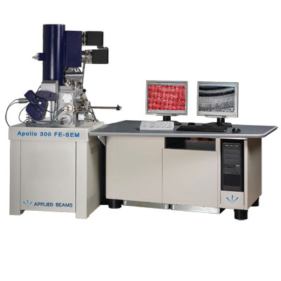
From optics to nanomaterials, solar panels and electronic devices, our SEM and AFM tools provide the resolution you need to understand the intimate details of your sample. Our staff are dedicated to help you get the results you need on time.
Contact Us to learn more how our unique set of FIB, SEM and AFM tools can meet your needs.

