
Our unique HyperFIB tool, utilizing plasma focused ion beam (FIB) technology for maximum beam currents and fastest material removal rates, offer unparalleled means to analyze your device or material.
Why a focused ion beam?
A focused ion beam can be thought of as an "atomic sand blaster". Our systems direct very high velocity ions toward the substrate to be machined, leaving behind a modified surface, hole, or pattern. Ion beams remove material through a process called sputtering; a ballistic process that removes material similar to a bowling ball knocking down pins. We digitally scan the ion bean across the material to be machined, creating 2D and 3D structures according to your design.
The advantages of plasma FIB for micro-machining:
What we need from you:
|
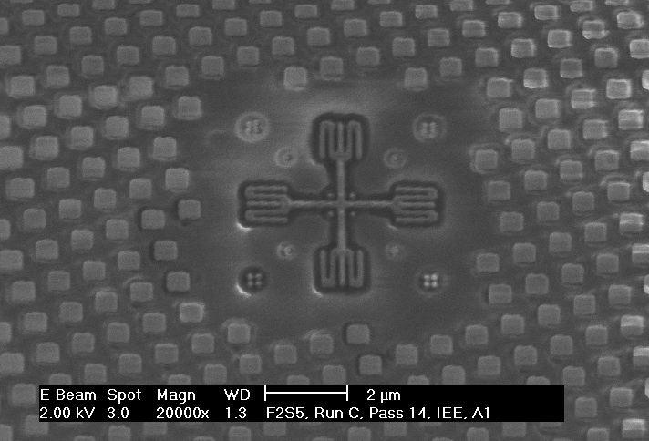
Delayer a complete integrated circuit Yes, the entire die. Full die delayering can help you answer critical questions relating to device design, piracy, counterfeiting, IP and patent infringement, and electrical failure analysis. We offer the unmatched ability to analyze device structures and layout by cleanly removing layers with multiple materials across an entire die, and provide high resolution images of your device. |
Full Die Delayering with HyperFIB |
Cross-section BGA solder balls, MEMS printheads, gold wires, stacked die and even printed circuit boards to uncover critical features and explore failure mechanisms. Machine unique features of centimeter size or larger, 300X faster than a Ga FIB, 20X more precise than a laser.
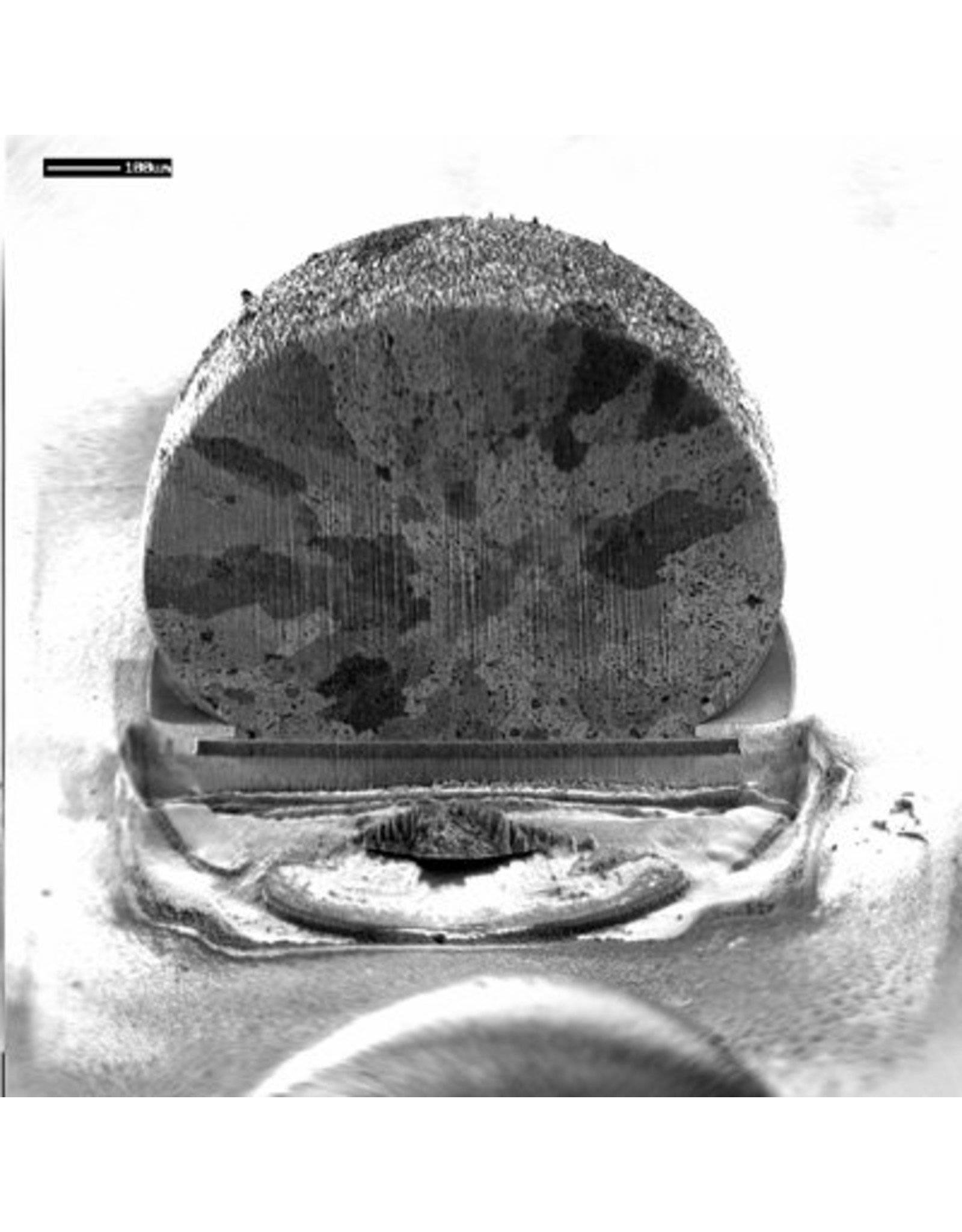
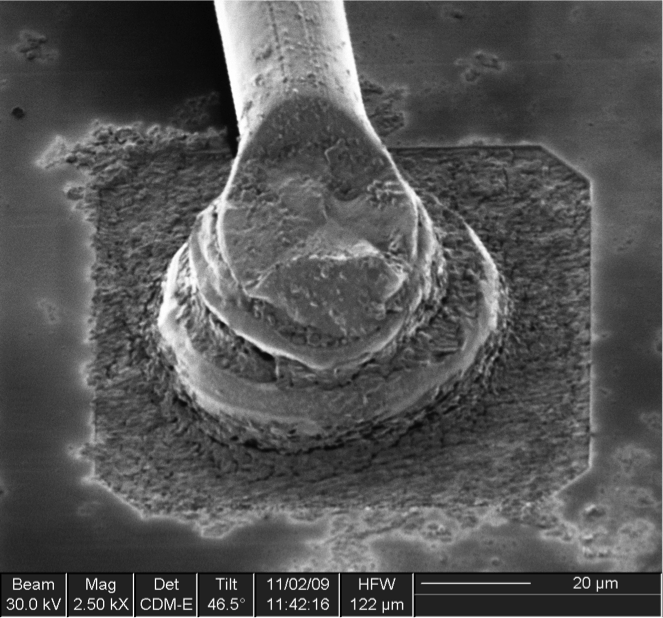 Failing Au wire bond Failing Au wire bond |
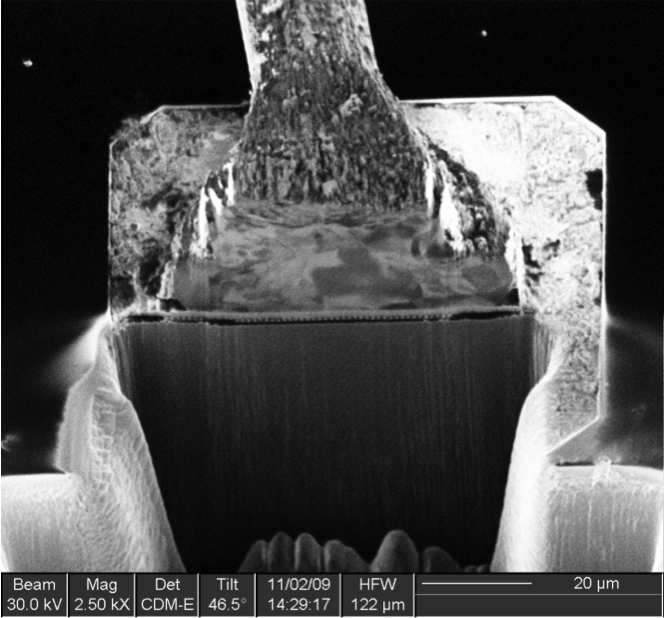 Wire bond sectioned and imaged with HyperFIB revealing contact void. Wire bond sectioned and imaged with HyperFIB revealing contact void.Total time to image < 1 hour |
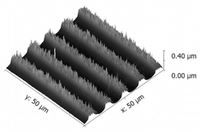
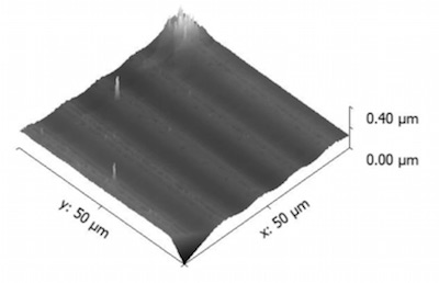
HyperFIB also exhibits the unique ability to shape and smooth surfaces over large and small areas. As a micromachining tool, HyperFIB is scanned over the sample surface using the patterning capability of modern FIB systems. HyperFIB and our unique scanning methods can remove surface roughness after just a few minutes of beam exposure. This capability is very useful for generating a smooth surface for optical components and for cleanly delayering integrated circuit devices.
|
AFM image of device surface as received, follows chemo-mechanical polishing step. |
AFM image post HyperFIB polishing. |
| In this example we use the high current available with HyperFIB to quickly refurbish worn probe tips used for electrical test. In <2 minutes per tip, HyperFIB is able to clean, re-shape and re-size these tips and put a non-functional probe card back to work. | 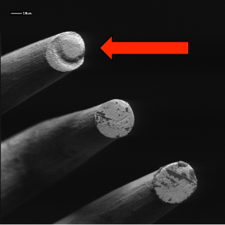 |
Have a unique micro-machining application?